Home / Research / Laboratories / Laboratory of SEM microscopy: LAB-SEM


The LAB-SEM is a CIO facility. External users could also have access to this lab previous petition.
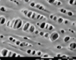
Scanning Electron Microscope was developed in 1937 by Manfred von Ardenne and uses an electron beam instead of light to form, visualize and analyze an image. It has a very deep field that enable to focus a large sample zone. It permits to analyze high resolution images (of only nanometers, 1 nm = 10-9 m) in such way that nanoscopic details can be visualized with large amplification (until 1 000 000 X). Sample preparation is relatively easy of performing.
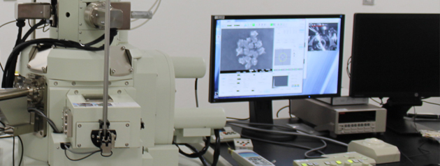
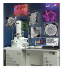
This new SEM equipment (model JSM-7800F from Jeol), unique at CIO and, one the best SEM in Mexico, is a device of emission field of high resolution capable to form and analyze images of only few nanometers in size till several microns. The maximum sample size possible of analyzing is 10 cm2 × 5 cm.
STEM (Scanning Transmission Electron Microscopy): Transmission images
EDS (Energy Dispersive X-ray spectroscopy): Chemical composition
Lithography through electrons: lithographic recording
Dr. José-Luis Maldonado-Rivera
e-mail: jlmr@cio.mx
Building D, Room 620
Phone: +52 (477) 441 4200 ext. 291
Last Update: Nov 17, 2022


Loma del Bosque 115, Lomas del Campestre León, Guanajuato, México. Zip Code 37150.
Phone +52 (477) 441 42 00-Fax +52 (477) 441 42 09
©2016 All rights reserved
